

Skip to content

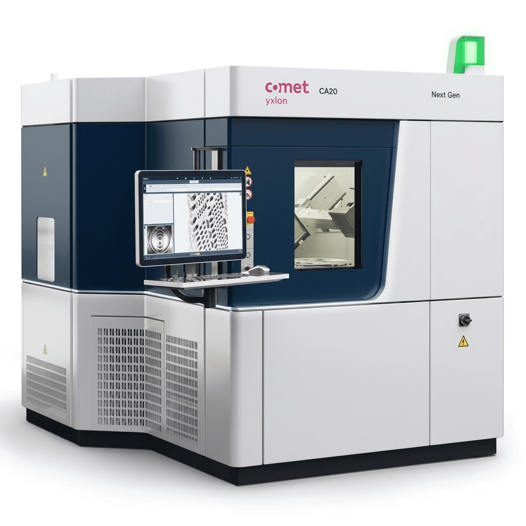
CA20

  • Designed to cover the entire semiconductor manufacturing chain, from wafer processing to packaged chips
  • Available with fully automated operation for seamless integration into your fab
  • AI-based data analysis and advanced software ensures fast, accurate defect classification to resolve systematic issues and maximize yield
  • Non-destructive technology for three-dimensional insights into solder bumps or TSVs within minutes
  • Repeatable results through reliable and accurate technology, designed to support a stable inspection routine
  • Cleanroom ready, with conditions within the cabinet comparable to ISO Class 3


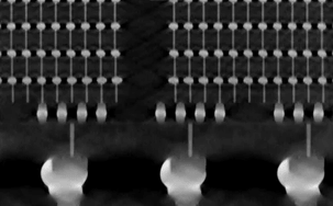
A 2D Slice taken from a 3D X-ray (CL) scan of a commercially available GPU.


CA20 inspection applications in R&D and production

  • Chip-on-Substrate including Fan Out packaging solder connections (C4 bumps and copper pillars)
  • 2.5 and 3D IC package solder connections including microbumps
  • TSV inspection
  • Substrate strip solder bumps
  • Sensors
  • MEMS and MOEMS

Product Enquiry

whatsapp-icon icon-chat