
- Detectable Defects
Particles, missing patterns, scratches, residues, contamination, pattern adhesion, etc. - High-precision 3D Optical Imaging System
Specifically developed for advanced packaging, ensures accurate and stable inspection results. - AI Algorithm
Integrates with latest generation of AI intelligent detection algorithms, requiring only a small number of images of good products for model training. This facilitates AI deployment and is convenient and efficient. - Optical Hardware
High-resolution industrial area scan camera, microscope optical system, 4-wheel nosepiece, equipped with 2x, 5x, 10x, and 20x microscope objectives, minimum pixel resolution 0.225 μm - Data Indicators
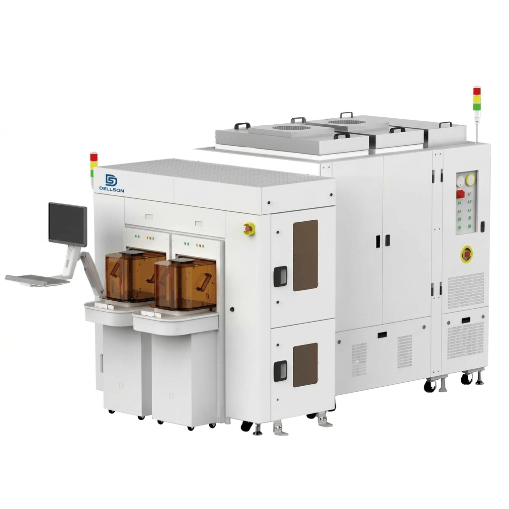
Supports 8/12-inch bare wafers, ring wafers, microporous ceramic X/Y/R, wafer stages, dual Foup automatic loading, automatic optical focus, automatic position correction, and automatic objective lens switching. - Advantages
A 100% integrated 2D and 3D measurement and inspection system capable of measuring bumps as small as 2µm in height. Patented reflection suppression technology allows inspection of highly reflective surfaces.

Inspects solder joints and component quality after wave soldering to ensure defect-free assembly and long-term reliability.